- 您现在的位置:买卖IC网 > Sheet目录1994 > DS3105LN+ (Maxim Integrated Products)IC TIMING LINE CARD 64-LQFP
DS3105
111
Table 10-6. LVPECL Level-Compatible Output Pins
(VDD = 1.8V ±10%; VDDIO = 3.3V ±5%, TA = -40°C to +85°C)
PARAMETER
SYMBOL
CONDITIONS
MIN
TYP
MAX
UNITS
Differential Output Voltage
VODPECL
595
700
930
mV
Output Offset (Common Mode) Voltage
VOSPECL
25
°C (Note 1)
0.8
V
Difference in Magnitude of Output
Differential Voltage for Complementary
States
VDOSPECL
50
mV
Note 1:
With 100
load across the differential outputs.
Note 2:
The differential outputs can easily be interfaced to LVDS, LVPECL, and CML inputs on neighboring ICs using a few external
passive components. See App Note HFAN-1.0 for details.
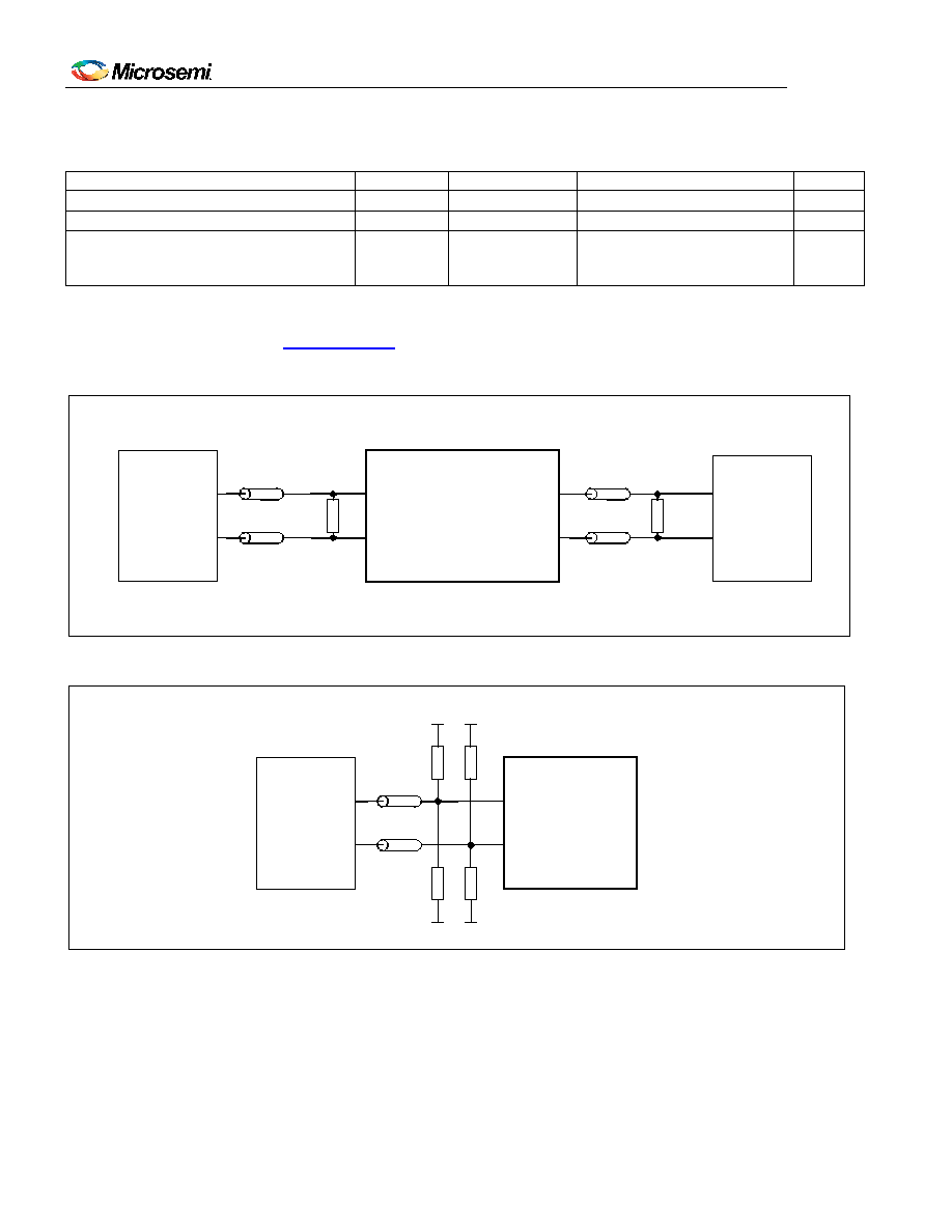
Figure 10-1. Recommended Termination for LVDS Pins
DS3105
LVDS
I/O
ICnPOS
ICnNEG
100
(5%)
50
OC6POS
OC6NEG
50
100
(5%)
LVDS
DRIVER
LVDS
RECEIVER
Figure 10-2. Recommended Termination for LVPECL Signals on LVDS Input Pins
DS3105
LVDS
INPUTS
ICnPOS
ICnNEG
130
82
50
GND
3.3V
LVPECL
DRIVER
发布紧急采购,3分钟左右您将得到回复。
相关PDF资料
DS3106LN+
IC TIMING LINE CARD 64-LQFP
DS3231MZ+
IC RTC I2C 8SOIC
DS3231SN#T&R
IC RTC W/TCXO 16-SOIC
DS3232MZ+
IC RTC W/SRAM I2C 8SOIC
DS3232SN#T&R
IC RTC W/TCXO 20-SOIC
DS3234S#
IC RTC W/TCXO 20-SOIC
DS32C35-33#T&R
IC RTC ACCURATE I2C 3.3V 20-SOIC
DS3911T+
IC DAC 10BIT I2C QUAD 14TDFN
相关代理商/技术参数
DS3106
制造商:MAXIM 制造商全称:Maxim Integrated Products 功能描述:Line Card Timing IC
DS3106A10SL3S(621)
制造商:Amphenol Corporation 功能描述:
DS3106A14S2S
制造商:Amphenol Corporation 功能描述:
DS3106A14S2S(621)
制造商:Amphenol Corporation 功能描述:
DS3106A14S5P
制造商:Amphenol Corporation 功能描述:
DS3106A14S5P(621)
制造商:Amphenol Corporation 功能描述:
DS3106A14S5S(621)
制造商:Amphenol Corporation 功能描述:
DS3106A14S6P
制造商:Amphenol Corporation 功能描述: